Rust Embedded: Light Sensor - Part 1
I wanted to build a little project where I could use the ADC of the STM32F303VC microcontroller. I came up with the idea to read values from a light sensor. So the light sensor is connected to the microcontroller via pin 0 of port A. We need to convert the voltage on this pin to digital values. That is where the ADC comes in - we convert from analog to digital.
Here is how I set it up:
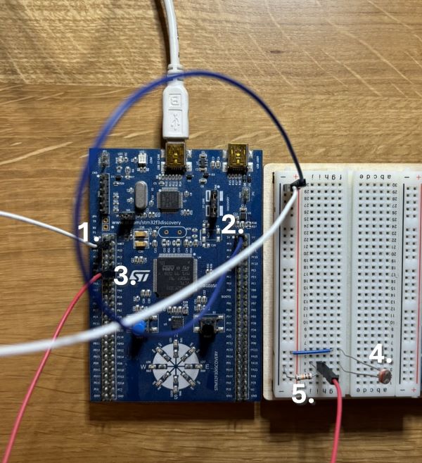 Board setup with light sensor
- connect the white cable to the GND pin on the board -> to the vertical - lane on the breadboard
- connect the blue cable to the 5V pin on the board -> to the vertical + lane on the breadboard
- connect the red cable to the PA0 pin on the board -> to the horizontal lane where the light sensor and the resistor are connected
- connect the light sensor via the blue connector on one side to the + lane -> the oder side via the resistor to the - lane
- connect the resistor (10k Ohm) to the - lane
Code on GitHub.
Here is the full code example for our program with the light sensor. I wanted to start bare-metal by only using the standard stm32f303 crate. Further down we’ll go through the code in more detail. After that, I will show you a version with the stm32f3xx_hal crate.
#![no_main]
#![no_std]

extern crate panic_halt;

use cortex_m_rt::entry;
use cortex_m_semihosting::{self, hprintln};
use stm32f3::stm32f303;

#[entry]
fn main() -> ! {
    // You should see that in your openocd output
    hprintln!("Hello from Discovery");

    let peripherals = &stm32f303::Peripherals::take().unwrap();
    let cp = cortex_m::Peripherals::take().unwrap();

    let mut delay = cortex_m::delay::Delay::new(cp.SYST, 8_000_000);
    let rcc = &peripherals.RCC;
    let gpioa = &peripherals.GPIOA;
    let adc1 = &peripherals.ADC1;
    let common_adc12 = &peripherals.ADC1_2;

    // Configure Port A Pin 0

    // Set HSI clock on
    rcc.cr.write(|w| w.hsion().on());
    // Set Pin 0 to analog input
    gpioa.moder.write(|w| w.moder0().analog());
    // Set Pin 0 to floating (disable schmitt trigger)
    gpioa.pupdr.write(|w| w.pupdr0().floating());

    // Enable GPIO Port A clock
    rcc.ahbenr.write(|w| w.iopaen().enabled());
    // Enable ADC1 clock
    rcc.ahbenr.write(|w| w.adc12en().enabled());
    // Set ADC clock mode
    common_adc12.ccr.write(|w| w.ckmode().sync_div4());

    // Configure ADC1

    // Set single conversion mode
    adc1.cfgr.write(|w| w.cont().single());
    // 12bit data resolution
    adc1.cfgr.write(|w| w.res().bits10());
    // Select channel 1
    adc1.sqr1.write(|w| unsafe { w.sq1().bits(1) });
    // Set sample time
    adc1.smpr1.write(|w| w.smp1().cycles601_5());

    // Reset control register
    adc1.cr.reset();

    hprintln!("Enable vrs");
    // Enable voltage regulation sequence.
    // This has to be done before the calibration.
    adc1.cr.write(|w| w.advregen().intermediate());
    adc1.cr.write(|w| w.advregen().enabled());

    // Wait for the startup time of the ADC voltage regulator
    // see STM32f303 reference manual section 15.3.6
    delay.delay_us(80);

    hprintln!("Start calibration");
    // Start calibration
    adc1.cr.write(|w| w.adcaldif().single_ended());
    adc1.cr.write(|w| w.adcal().calibration());
    while adc1.cr.read().adcal().is_calibration() {
        hprintln!("hoho");
    }

    hprintln!("Disable vrs");
    // Disable voltage regulation sequence.
    adc1.cr.write(|w| w.advregen().intermediate());
    adc1.cr.write(|w| w.advregen().disabled());

    hprintln!("Enable adc");
    // Enable the ADC
    adc1.cr.write(|w| w.aden().enabled());
    while adc1.isr.read().adrdy().is_not_ready() {}

    hprintln!("Start loop");
    loop {
        // Start conversion and wait until ECO and EOS is set.
        adc1.cr.write(|w| w.adstart().start_conversion());
        while adc1.isr.read().eoc().is_not_complete() && adc1.isr.read().eos().is_not_complete() {}

        // Read data from data register
        let data = adc1.dr.read().rdata().bits();

        hprintln!("{}", data);

        // Wait 100ms for next conversion
        delay.delay_ms(100);
    }
}
Like always, we fist need to take the peripherials which gives us access to the RCC (register and clock control register), to the GPIOA (port A) and to the ADC1 (analog-digital converter). After that we can start to setup our system.
// Set HSI clock on
rcc.cr.write(|w| w.hsion().on());
// Set Pin 0 to analog input
gpioa.moder.write(|w| w.moder0().analog());
// Set Pin 0 to floating (disable schmitt trigger)
gpioa.pupdr.write(|w| w.pupdr0().floating());

// Enable GPIO Port A clock
rcc.ahbenr.write(|w| w.iopaen().enabled());
// Enable ADC1 clock
rcc.ahbenr.write(|w| w.adc12en().enabled());
// Set ADC clock mode
common_adc12.ccr.write(|w| w.ckmode().sync_div4());
First we activate the HSI clock which is an internal 8MHz RC oscillator that we’ll use as the system clock. Next we set pin 0 of port A as input and also set the pin as floating. By that we say “don’t set pin to HIGH or LOW on voltage change” - we just want the raw voltage that is applied to this pin from an external source. We enable port A by enabling the clock, we enable the ADC1 clock and set the ADC clock mode to HCLK/4 - which basically means “Take the rcc_hclk3 frequency and divide it by 4 — use that as the ADC clock.”. The rcc_hclk3 is the clock frequency for the AHB bus on which our GPIO port hang. For more details see section 9.2.8 and 9.4.6 in the reference manual.
// Set single conversion mode
adc1.cfgr.write(|w| w.cont().single());
// 12bit data resolution
adc1.cfgr.write(|w| w.res().bits10());
// Select channel 1
adc1.sqr1.write(|w| unsafe { w.sq1().bits(1) });
// Set sample time
adc1.smpr1.write(|w| w.smp1().cycles601_5());

// Reset control register
adc1.cr.reset();

hprintln!("Enable vrs");
// Enable voltage regulation sequence.
// This has to be done before the calibration.
adc1.cr.write(|w| w.advregen().intermediate());
adc1.cr.write(|w| w.advregen().enabled());

// Wait for the startup time of the ADC voltage regulator
// see STM32f303 reference manual section 15.3.6
delay.delay_us(80);

hprintln!("Start calibration");
// Start calibration
adc1.cr.write(|w| w.adcaldif().single_ended());
adc1.cr.write(|w| w.adcal().calibration());
while adc1.cr.read().adcal().is_calibration() {
    hprintln!("hoho");
}

hprintln!("Disable vrs");
// Disable voltage regulation sequence.
adc1.cr.write(|w| w.advregen().intermediate());
adc1.cr.write(|w| w.advregen().disabled());

hprintln!("Enable adc");
// Enable the ADC
adc1.cr.write(|w| w.aden().enabled());
while adc1.isr.read().adrdy().is_not_ready() {}
Next we need to configure the ADC1 by setting some values like the conversion mode, the data resolution, channel and the sample time. After that a very important step begins. The voltage regulation sequence. How this works and what has to be done can be found under 15.3.6 ADC voltage regulator of the reference manual. So first the voltage regulation is enabled. After that the calibration can be started - with the while loop we wait until the calibration is done. When done we can disable the voltage regulation and finally can enable the ADC. Again, we need to wait until the ADC is ready with a while loop.
hprintln!("Start loop");
loop {
    // Start conversion and wait until ECO and EOS is set.
    adc1.cr.write(|w| w.adstart().start_conversion());
    while adc1.isr.read().eoc().is_not_complete() && adc1.isr.read().eos().is_not_complete() {}

    // Read data from data register
    let data = adc1.dr.read().rdata().bits();

    hprintln!("{}", data);

    // Wait 100ms for next conversion
    delay.delay_ms(100);
}
Now we can start our loop and read data from our input pin. Of course a light sensor needs to be attached to our microcontroller. If you flash the program and everything is setup correctly, you should see the numbers in your terminal output change if the light over the sensor changes. Eg. if you hold your hand above or an light source - so going from dark to light.
On to Part 2 -> Rust Embedded: Light Sensor - Part 2